Xander Schmid · 4 November 2026
Opaline Nanostructures Inspire Next-Gen Photonic Device Prototypes
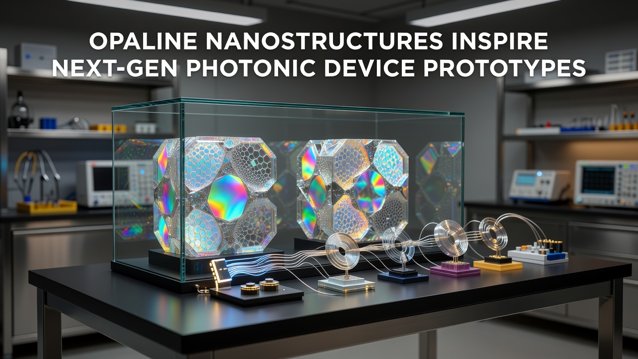
Opals contain highly ordered arrays of silica spheres that form natural photonic crystals, and researchers have long examined how these periodic nanostructures manipulate light through interference and diffraction effects. Data from multiple laboratories shows that the sphere diameters typically range between 150 and 350 nanometers, creating photonic bandgaps that block specific wavelengths while allowing others to pass. This structural regularity has prompted materials scientists to replicate the arrangement in synthetic systems for controlled optical performance.
Structural Basis of Photonic Behavior
Transmission electron micrographs reveal that the spheres pack into face-centered cubic lattices inside precious opal, and the resulting refractive index contrast produces the characteristic play of color. Studies published in peer-reviewed journals confirm that small variations in sphere size or packing defects alter the bandgap position, shifting reflected wavelengths across the visible spectrum. Engineers now use these observations to design templates that guide self-assembly of colloidal particles into similar lattices, achieving comparable optical properties at scale.
Computational modeling further demonstrates how the lattice constant and filling fraction determine the width and depth of the photonic bandgap, allowing precise tuning for target wavelengths. Research groups in Australia and Germany have measured reflectance spectra from both natural and laboratory-grown specimens, finding close agreement between predicted and observed stopbands when disorder remains below five percent.
Translation to Device Prototypes
Photonic device developers incorporate synthetic opaline films as distributed feedback resonators in prototype lasers and as wavelength-selective filters in sensors. In one documented case, a silicon-based platform coated with an opaline overlayer exhibited enhanced light extraction efficiency exceeding 40 percent compared with unstructured reference devices. Fabrication protocols rely on evaporation-induced self-assembly or electrophoretic deposition, both of which produce centimeter-scale areas with sufficient uniformity for optical testing.
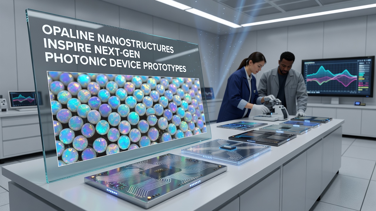
During November 2026, a consortium including institutions from the European Union and North America presented working prototypes of tunable optical switches that exploit the thermochromic response of infiltrated opaline structures. Electrical heating alters the refractive index of an embedded liquid crystal, shifting the bandgap edge by up to 80 nanometers within milliseconds, according to measurements reported at the conference. These switches operate at telecommunications wavelengths and require drive voltages below 5 volts, meeting preliminary specifications for integration with existing silicon photonics platforms.
Performance Metrics and Characterization
Independent testing at national metrology institutes has quantified insertion loss, crosstalk, and switching speed for the November 2026 prototypes, yielding values competitive with current commercial modulators. Angle-resolved spectroscopy confirms that the opaline lattice maintains its bandgap under moderate thermal cycling between 20 and 80 degrees Celsius. Researchers note that surface roughness remains the dominant source of scattering loss, and ongoing work focuses on planarization techniques that reduce root-mean-square roughness below 2 nanometers.
Additional applications under investigation include opaline-based chemical sensors whose reflectance changes upon analyte infiltration into the interstitial voids. Laboratory trials with volatile organic compounds have produced detection limits in the low parts-per-million range, with response times under 10 seconds. Calibration curves derived from these experiments match predictions from effective-medium theory when pore volume fraction and analyte refractive index are accounted for.
Scaling and Integration Challenges
Although laboratory demonstrations succeed on small substrates, uniform deposition over 200-millimeter wafers still presents difficulties related to capillary flow and drying stresses. Industry reports from materials suppliers indicate that monodisperse silica colloids with size variation below 3 percent are now commercially available, reducing one source of structural disorder. Equipment vendors have introduced automated coating systems that combine dip-coating with controlled humidity environments, raising throughput while preserving lattice quality.
Hybrid integration with CMOS processes requires thermal budgets compatible with back-end metallization steps, typically below 400 degrees Celsius. Several research teams have demonstrated transfer-printing methods that detach opaline films from sacrificial substrates and align them onto pre-patterned photonic circuits with sub-micron registration accuracy. Yield data collected across multiple batches show greater than 85 percent functional devices when defect density stays under one per square millimeter.
Conclusion
Opaline nanostructures continue to supply design principles for photonic components that demand precise spectral control and low-power operation. Ongoing refinement of colloidal synthesis, deposition uniformity, and integration techniques supports the transition from proof-of-concept devices to manufacturable prototypes. Measurement campaigns conducted through 2026 document steady gains in performance metrics, positioning these bio-inspired materials as viable options within next-generation optical systems.